


Schedule a Call Back


ISRO selects Hind High Vacuum for supplying thin film metallised circuit
 Industry News
- Sep 24,18
The Bengaluru based HHV will produce the entire thin film metallised circuit for ISRO’s satellite program

Bengaluru, September 24, 2018
ISRO has selected the Bengaluru based Hind High Vacuum Co Pvt Ltd (HHV), a vacuum science and technology company, under its technology transfer program. HHV will produce the entire thin film metallized circuit for ISRO’s satellite program.
In 2017, HHV was awarded a ‘Certification of Qualification’ by the Space Application Center, ISRO for thin film metalized substrates. Circuits are designed on these multi-layered metallised substrates and used in ISRO’s space and satellite program. This indigenously developed technology, as a part of HHV’s ‘Make in India’ initiative, was recognised by the Government of India and the company was conferred with the prestigious National Research & Development Award in May, 2018.
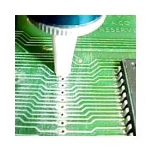
“As a part of ISRO’s technology transfer program and as a forward integration of this award winning technology, HHV will now produce the entire thin film metallised circuit (TFMC) for ISRO’s 40-micron accuracy line, in its new technology production line known as ‘Photo Lithography’. HHV has established a new Photo Lithography Lab (PLL) at its Dabaspet plant to develop TFMCs on alumina substrates that first need to be metallised in a vacuum chamber,” said Prasanth Sakhamuri, Managing Director, HHV.
Once metallised these substrates are cleaned and then coated with a photo resistive material using a spin coater. A laser writer is used to define different designs as required by customers on blank chromium mask plates. Once covered with a patterned mask plate the substrates go through ultra-violet exposure to harden exposed areas. HHV uses positive lithography to pattern and etch the metallised substrates.
A specialised etching room containing a chemical wet bench is used for multiple rounds of etching for each metallic layer. A dicing machine is then used to cut the metallised substrates to required sizes and an ISO 8 clean room is used to qualify the products. High performance microscopes and profile projectors are available for the inspection and measurement of the patterned substrates.
“The entire process requires high levels of precision and sophisticated technology to deposit coatings pattern the circuits and check the quality of the substrates within a 1000th of a millimetre. All these processes require clean room environments to ensure minimal interference with particle matter present in air. HHV’s Photo Lithography Lab has ISO 7 and ISO 8 clean rooms as well as class 100 laminar flow stations that allow us to achieve resolutions of up to 40 microns” added Prasanth Sakhamuri.
Established in 1965 at Bangalore as a specialised enterprise to develop Indian self-reliance in high vacuum technology, HHV today serves a spectrum of industries and R&D centres covering aerospace, atomic energy, defence, automotive, semi-conductors, electrical, horology, scientific instrumentation, decorative, food processing to name a few. HHV has an advanced research and manufacturing program in thin film technology, material science, metallurgy, astronomy, and special purpose machinery.
Hind High Vacuum
HHV
ISRO
Prasanth Sakhamuri
satellite
aerospace
atomic energy
defence
automotive
thin film metallised circuit
Make in India
Related Stories
Auto & Auto Components

Minda Corp, Toyodenso Form JV for Automotive Switches
The joint venture will set up a greenfield facility in Noida (Uttar Pradesh) with operations expected to commence in the second half of FY 2026–27
Read moreAuto & Auto Components
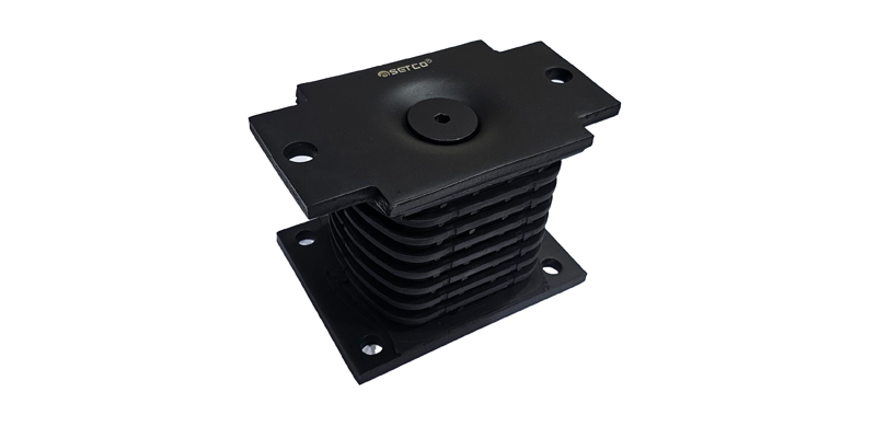
Setco Automotive launches load cushion and torque rod bush
Designed to perform in challenging conditions, these suspension components are engineered to enhance vehicle stability, ride quality, and shock absorption.
Read moreProcess Equipment

We see strong demand for process equipment in next 5 years: Shalabh Singh
in this exclusive conversation with Rakesh Rao, Shalabh Singh, Chief of Business Development at Isgec Heavy Engineering Ltd, delves into how Isgec is aligning itself with national priorities while t..
Read moreRelated Products
Plated Through Holes
Printed Circuits and Integrated Circuits
Anand Electronic Circuits offers a wide range of Plated Through Holes. This circuits are printed and integrated.
Read more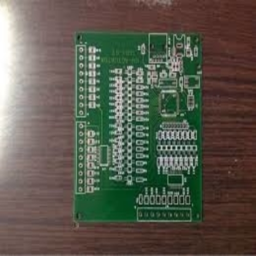
Printed Circuit Boards
Printed Circuits and Integrated Circuits
Anand Electronic Circuits offers a wide range of Printed Circuit Boards. They offer a wide range of Printed Circuit Board used to support electrically connect electronic components. Made Read more
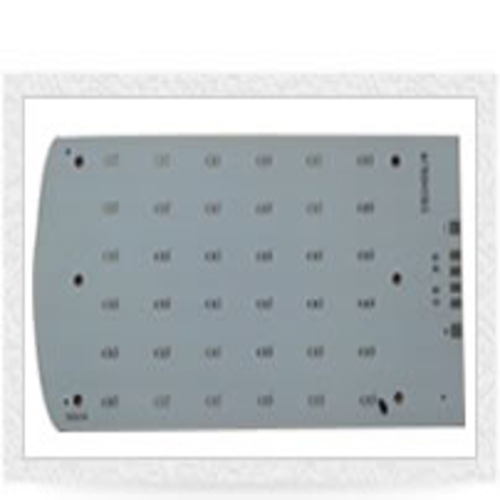
Aluminum Metal Core PCB
Printed Circuits and Integrated Circuits
Acme Circuits offers a wide range of Aluminum Metal Core PCB.
Read morelatest News
Subscribe to iNoW
For Industry News on WhatsApp, Give a Miss Call on: +91 84228 74016