


Schedule a Call Back


LED Packing Technology
 Technical Articles
- Nov 28,13
NULL

 Light Emitting Diodes [LEDs] are currently the most energy efficient and futuristic lighting sources for mankind. The demand for LED lighting applications is growing exponentially. This article discusses a few technical issues in manufacturing LEDs, also called Packaging of LEDs starting with LED semiconductor chips.
The group III-V compounds have electron energy band gap falling in the visible light region. The Indium Gallium Nitride (InGaN) multilayer epitaxial layered pn diodes emit the most efficiently in 450 nm (blue) by way of the process called electroluminescence [EL]. Part of this monochromatic light is converted to yellow and red colour by applying suitable phosphor coating of right thickness in the epoxy lens and resultant light is seen as white light. This type white LED is also called PCLED.
Unlike incandescent bulbs where only 3% of the total power is emitted as light, in case of LEDs, which are 12 time more efficient, nearly 35% of the power expended is emitted as light. The balance 65% of power is manifested as heat within the LED and same has to be conducted out to atmosphere smoothly, to let the LED continue to work at its best efficiency.
Modern LED packages reduce the thermal resistance dramatically. In LEDs life is enhanced by 20000 hrs with a ten degree temperature reduction.
 The thermal resistance of the LED is determined by the effective heat removal design of the LED manufacturer. An efficient thermal engineering of the package can also help in reducing the device dimensions thus greatly improving the future scalability of these devices. The thermal resistance of the package needs to be sufficiently low if the advantages obtained at die level are to be maintained at module level.
Modern power LED with added heat slug for enhanced evacuation of heat from the LED chip

Hence selecting the substrate material, thermal interface to the heat sink, or other cooling methods to ensure the device is operating reliably within the expected ambient temperature range.
Traditional LED Packages
Currently, Polyphthalamide (PPA) is the major lead-frame material for packaging low-power chips. The ceramic and Liquid Crystal Polymer (LCP) are primarily used for high-power packages. While ceramic has a good melting point, the ceramic-based lead frame, like PPA and LCP lead frames, has to be made with tooling, hence limiting the frame reduction to miniaturisation micron scale. However, a PPA lead frame, for instance, can be miniaturized to 3 mm long by 1.4 mm wide at best, holding a 9-mil (0.225 sq.mm) LED chip.
Silicone Large Wafer Technology Experience

Use of silicon wafers to grow GaN LEDs could lead to drastic fall in cost of LEDs, once uniformity across 12" area is mastered. Silicon has an excellent heat resistance (see graph). Si has best suited coefficient of thermal expansion (CTE). Silicon melts at 1,000 C, its CTE or coefficient of thermal expansion is below 4 ppm/C, and its TC or thermal conductivity is in the 150-180 W/m.k.
In near future, one can build LED driver ICs also into the WLP LED package by etching circuits on the bottom of the silicon lead frame, thereby shrink the size of LED modules into a miniscule.
Challenges in the Packaging of GaN-on-Si Devices

Direct growth of GaN-on-Silicon substrate is one of the good options to get rid of Sapphire. Yet this will require the reuse of mainstream technologies such as leadframe and wirebond packaging. This is because, GaN-on-Si devices for LED applications require Si substrate removal since light is emitted in the same direction as the substrate. It is a technology challenge for substrate transfer to get the GaN film effectively flipped and electrically connected.
Wafer-level Packaging

This brings us to option of growing GaN on traditional way, then removing them by LLO (laser lift-off technology) and then transferring it to Silicone substrate using wafer to wafer processes to derive complete package there itself. Wafer-level packaging and advanced technologies such as Through-Si Vias (TSVs) could offer a solution: they could provide effective means of substrate transfer and allow wafer-level integration of some more packaging elements like optics and drivers.
Among the cost of ceramic packaging is the highest whereas WLP is the cheapest, with PPA and LCP in the middle. If a ceramic package costs US$0.25, a PPA would be around US$0.06, an LCP would be around US$0.08 and WLP would be around US$0.03.
LED Bonding Process

1. Die Attach Process also known as Die Bond or Die Mount, is the process of attaching the LED chip to the die pad of the lead frame of the package. There are three main stages: First, the adhesive is dispensed on the die pad. Next, the die must be ejected from the wafer tape. A push-up needle pushes upward on the die backside to dislodge the die off the wafer tape. Third, a pick-and-place tool picks the die from the wafer tape and positions it on the adhesive.
The key factors are:
- The amount of the adhesive: Although the junction high is 75~145?m, too much adhesive will cause the p-n junction short
- Dimension of push-up needle: should fit the chip with tip radiun as 0.25~0.6 mm only, and
- Pick-and-place of the LED chip is achieved by either antistatic plastic tool which is made of rubber, though tools made of hard materials like tungsten carbide, ceramic, or steel, are also popular.
Alternate is eutectic bonding, achieved by low melting alloy like gold-zinc alloy is used to affix LED chip to silicon lead frames. While, epoxy glues used in most LED packages melt at 180?C, Eutectic bonding is much better in thermal resistance and does not absorb the emitted light in the package during high temperatures as epoxy. Here to prevent the high melting temperature from destroying the lead frame construction during the bonding process, the LED chip is first bonded on a heat-resistant board and then the board is adhered to the lead frame (ref Cree).

2. Wire Bond Process comprises of using the gold ball bonding as electrical connection. A gold ball is first formed by melting the end of the wire through electronic flame-off (EFO). Then free-air ball is brought into contact with the bond pad on the chip. The bonder applies pressure, heat, and ultrasonic forces to the ball, forming the metallurgical weld between the ball and the bond pad. Then the wire is run to the lead frame, forming a loop between the bond pad and the lead frame. Pressure and ultrasonic forces are applied to the wire to form the second bond. Bonding force of first bond should be fine tune to prevent the stress damage the bond pad and chip.
One can substitute both DieBond and WireBond steps with one step flip chip bonding technique in large chips of high power.
Encapsulation Process

The encapsulation of bonded LED Chips not only provide protection from ambience but also help in shaping of the out beam, be it Lambertian, focussed, batwing, etc. The lifetime of LED is not only due to the chip, but also the encapsulation materials and phosphor material. The silicone resins are expensive but far superior to epoxies.
In solid-state white lighting technology, phosphors are applied to the LED chip in such a way that the photons from the blue gallium nitride LED pass through the phosphor, which converts and mixes the blue light into the green-yellow-orange range of light. When combined evenly with the blue, the green-yellow-orange light yields white light. The notion of multiple colours creating white may seem counterintuitive. While in reflective pigments, mixing blue and yellow yields green; with emissive light, however, mixing such complementary colours yields white.
LED testing - In LED manufacturing processes, normal variations in the brightness and exact colour LED die and variations in the phosphor coating processes during die packaging lead to variation in the brightness and the "whiteness" of manufactured PCLEDs. During final testing, these LEDs are sorted into different intensity and colour bins. Within one intensity bin, some PCLEDs will be a bluer white, others a yellower white, and so on. LED manufacturers need to find applications for each of these bins to keep manufacturing costs under control. The most popular LEDs are
Here are Few Issues of Importance to Application of LEDs

ESD Protection - All InGaN chips are prone to electrostatic discharge (ESD) damage. And the equipments must be properly grounded and wrist bands or anti-electrostatic glove used when handling the chips. The non InGaN chips are robust to withstand ESD problems.
CRI - Another limitation of many PCLEDs stems from how coloured objects appear when illuminated by the type of white light they produce. A white light source's ability to accurately reveal colours depends on the number and intensity of the colours contained in the light coming from that source. The red or green objects aren't as vivid when illuminated by PCLED white light made from a mixture of blue and yellow light. New phosphors that can convert blue LED light to other wavelengths besides yellow are now being combined with YAG:Ce to improve the colour rendering of blue InGaN PCLEDs.

Another approach is to use UV emitting LEDs and a blend of phosphors that convert the UV into blue, green and red emission which combine to appear white. This approach improves colour rendering and can reduce manufacturing variability (range of whiteness) of the light made by the PCLED. Packaging UV LEDs presents more challenges for some of the packaging materials, including lower reflectivity of metal surfaces and mould compounds which reduces brightness and photo-degradation of epoxies and other plastic package parts which reduces LED lifetime. As with research on phosphors for use with LEDs, research on packaging materials better suited for use with UV InGaN LEDs is getting a lot of attention.
Kwality Photonics produces a range of power LEDs from 0.5 W up to 26 W. Kwality Photonics P Ltd, is an ISO 9001-2008, 25 years young company, a pioneer in India and No.1 maker of LEDs with fully indigenous technology involving R&D work at IISc, BARC, TIFR, NPL, CEL and in-house since 30 years.

The most popular are Polywa Power LEDs, 1 W KLHP331 series that emit 100-130 Lumens @ 350 mA and 180-240 Lumens @ 700 mA. Popular street lighting is KLHP3ST1WE PolyWa Oval LEDs with in-built lenses for street lighting applications having 80? x 130? viewing angle (right LEDs for street lights) to make it easy for the street light makers.
PLCC SMD LEDs, Super Flux LEDs and Straw-hat LEDs comprise the low power LED range from Kwality emitting 8 Lumens, the industry best. All the low power LEDs deliver exceptional brightness thanks to the specially designed lead frame profile. The SMD 3528, 2835 and 3014 are ideal for smooth glow LED tube lights. These PLCC SMD LEDs are offered in a range of colours with typical luminous flux varying from 8 Lumens @ 20 mA, 12 Lm@30 mA and 24 Lm@60 mA.
Kwality PolyWa 5630 Series are embedded with single large chip capable of being driven up to 150 mA to obtain 60-65 Lm. The PolyWa 5630 are ideal for retrofit bulbs and down light applications. This KLSL5630W SMD LED is currently India's most affordable LED, and helps the LED lamp maker to achieve their dream costs. COB LED modules have multiple chips in one cluster to increase in 5, 7, 9 and 50 W range and produce 90 to 100 Lumens per watt rating
Kwality produces LED segment displays of single and multiple digit seven segment, dot-matrix, light bars, bar graph, arrow displays and jumbo digits, in red, green, amber, yellow, ultra green, blue and white emission. The displays size varies from 0.3" to 12" in glow area. These LED displays enjoy highest popularity since 2 decades.
About the Author
K Vijay Kumar Gupta, BSc & BE, is Managing Director, Kwality Photonics P Ltd, Hyderabad. He is Past President ELCINA, ELIAP and Member BIS23/24, ELCOMA-BEE Standards, Advisor - DEITY (Opto & Materials) R&D Review Committees. He has 35 years experience in LED technology field at IISC, BARC, TIFR and CEL/NPL/DST and with the Kwality Group of Industries. Email: econoredledskwality@gmail.com
Related Products

Liquid Ring Vacuum Pumps/Compressors
Compressors and Allied Equipment
Aeromatic Engineering Private Limited offers a wide range of liquid ring vacuum pumps/compressors.
Read more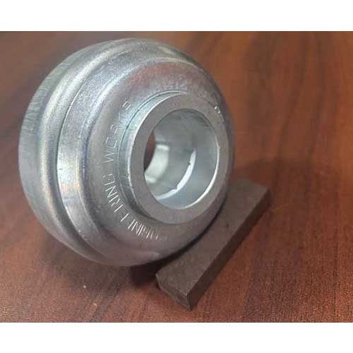
Hot Wheel Bearing
Bearings, Bushings, Wheels and Gears
SICCO Engineering Works offers a wide range of hot wheel bearing. Read more
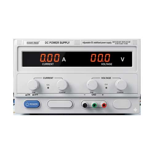
Kusam-meco DC Power Supply Model Km-ps-3020 Abf / Km-ps-3030 Abf
Power Supplies, Batteries & Accessories
<p>Kusam Electrical Industries Ltd offers Kusam-Meco DC power supply model KM-PS-3020 ABF/ KM-PS-3030 ABF</p> Read more
latest News
Subscribe to iNoW
For Industry News on WhatsApp, Give a Miss Call on: +91 84228 74016