


Schedule a Call Back


TRUMPF Showcases Laser and Plasma Technologies at Semicon Japan 2025
 Articles
- Dec 18,25
At Semicon Japan 2025, high tech company TRUMPF demonstrates how innovative laser and plasma technologies can reduce production costs, improve chip quality, and make the semiconductor industry fit for the future.

At Semicon Japan 2025, high tech company TRUMPF demonstrates
how innovative laser and plasma technologies can reduce production costs, improve
chip quality, and make the semiconductor industry fit for the future. “The semiconductor
industry is growing rapidly and faces the challenge of combining efficiency,
precision, and sustainability. At Semicon Japan 2025, we will show how our
technologies and services meet these requirements. Our technologies form the
basis to produce the latest generation of microchips, which are needed for AI
applications, for example,” said Michael
Samtleben, Managing Director of TRUMPF in Japan. At the trade fair, the
high-tech company will present a combined laser etching process for the latest
generation of microchips and a new generation of its high[1]frequency power
supplies with the TruPlasma RF Series G3.
Laser process enables
cost-effective high-speed chips
Advanced packaging with glass is a crucial future technology
for the semiconductor industry. Glass is significantly cheaper than silicon.
This allows manufacturers to reduce production costs and makes high-performance
end devices much more affordable for customers. In Advanced Packaging, chip manufacturers
combine individual chips on interposers, a thin intermediate layer that
electrically connects the individual chips.
To create connections on the interposer, chip manufacturers
must drill holes in the glass, known as through[1]glass
vias (TGV). Manufacturers often have to drill millions of holes in a panel to create
the required connections. TRUMPF laser technology can play an important role
here. An ultrashort pulse laser from TRUMPF can selectively change the
structure of the glass, which is then treated with an etching solution. The
laser and etching processes must be perfectly coordinated to create precise holes.
TRUMPF has already proven that this is possible in a project with the SCHMID
Group, a specialist in etching processes for microchip production.
Beyond laser technology for TGV drilling, TRUMPF is
committed to addressing its advanced HiPIMS process (High Power Impulse
Magnetron Sputtering). This technology ensures extremely uniform copper coating
along the via sidewalls, which is a critical prerequisite for subsequent bulky
metallization process.
What sets TRUMPF apart? Its unique rectangular waveform
delivers ultra-high ionization energy, reaching almost twice the deposition
rate of other HiPIMS products available on the market. Additionally, it
achieves a highly conductive and denser copper film, far superior to that
produced by conventional DC sputtering, making it ideal for TGV applications.
Combined with synchronized bias technology and a fully integrated TRUMPF system,
HiPIMS ensures perfect copper filling even for extremely high aspect-ratio
vias. TRUMPF’s HiPIMS TGV solution can deliver excellent deposition precision
and highly reproducible process control.
With extensive industrialization experience alongside
leading manufacturers, TRUMPF is not only a generation ahead technologically
but also setting the market benchmark for high-volume TGV production. By
combining laser drilling and HiPIMS coating, TRUMPF paves the way for more cost[1]effective,
higher-performing chips and sets new standards in Advanced Packaging.
TRUMPF ensures more
precise plasma processes in chip manufacturing
TRUMPF
Semicon Japan 2025
laser technology
plasma technology
semiconductor industry
microchips
AI applications
laser etching
TruPlasma RF Series G3
Related Stories
Automation & Robotics

Global Motion Controls Market Set to Recover with 3.9 per cent Growth in 2026
After two years of decline, the global motion controls market is expected to return to growth in 2026, supported by APAC expansion and rising automation demand.
Read moreMachine Tools & Accessories

TRUMPF Launches High-Performance TruLaser Tube 7000 System
TRUMPF unveils the TruLaser Tube 7000, delivering higher productivity, precision, and flexibility in laser tube processing with advanced automation and digital services.
Read moreMachine Tools & Accessories
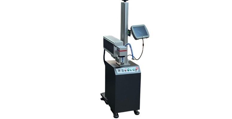
C and C Laser Engineering Pvt Ltd (CnC) delivers precision laser marking, engraving and processing systems for industrial and craft applications.
CnC offers advanced CO?, fibre and UV laser processing solutions
Read moreRelated Products
Precision Cutting Tools1
MACHINE TOOLS, POWER & HAND TOOLS
S S Trading Corporation offers a wide range of precision
cutting tools.
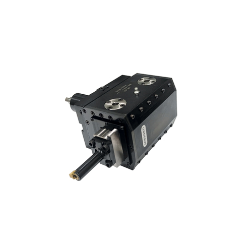
Slotting Head Unit for All Cnc Turn Mill Centers
MACHINE TOOLS, POWER & HAND TOOLS
Sphoorti Machine Tools Pvt Ltd offers a wide range of
slotting head unit for all CNC turn mill centers.
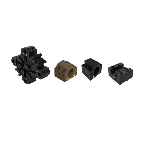
Slotted Tool Disc and Tool Holders
MACHINE TOOLS, POWER & HAND TOOLS
Prominent Machine Tools offers a wide range of slotted tool disc and tool holders.
latest News
Subscribe to iNoW
For Industry News on WhatsApp, Give a Miss Call on: +91 84228 74016