


Schedule a Call Back


New govt incentives to boost semiconductor manufacturing
 Industry News
- Jan 19,22
The proposed incentives are worth Rs 760 billion over the next six years and provides 25% incentives on capital expenditure for establishing unit of Compound Semiconductor Wafer Fabrication (FAB), assembly, testing, and packaging facility in the country.
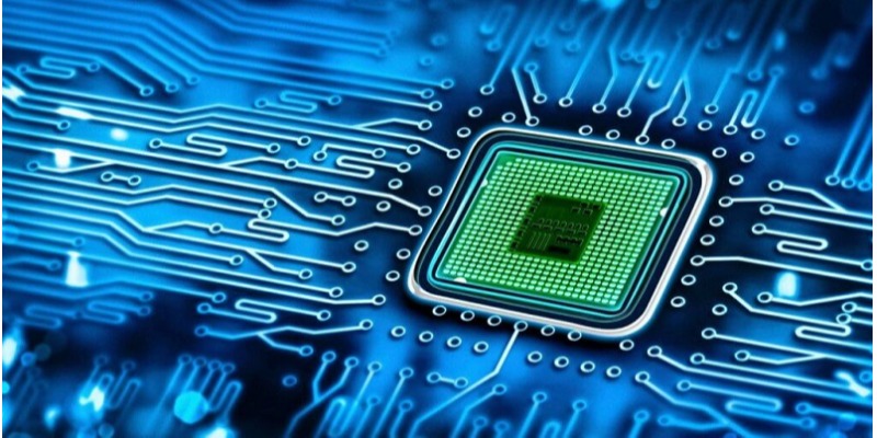
Last month, the Union Cabinet approved a comprehensive program - with an outlay of Rs 760 billion (about $ 10 billion) - for the development of sustainable semiconductor and display ecosystem in the country. Industry experts consider this to be a first towards making India a global hub for Electronic System Design and Manufacturing (ESDM).
“This is a huge positive step for the Indian electrical & electronics industry. This will accelerate our indigenisation efforts and enable global competitiveness of our industry to ramp-up exports of finished products,†said Vipul Ray, President, Indian Electrical & Electronics Manufacturer’s Association (IEEMA). He hailed it as one of the most significant moves towards realising the vision of Aatmnirbhar Bharat; one which has come at an opportune time to tackle the global shortage of Semiconductors. “It should help streamline the disrupted global supply chain and help mitigate the cyber security risksâ€Â, he added.

The new incentives are for every part of supply chain including electronic components, sub-assemblies, and finished goods. The program is expected to usher in a new era in electronics manufacturing by providing a globally competitive incentive package to companies in semiconductors and display manufacturing as well as design. This will pave the way for India’s technological leadership in these areas of strategic importance and economic self-reliance.
“Semiconductors are widely used in manufacturing of many electrical equipment, viz: smart energy meters, control & automation products, testing & measurement instruments and switching products, to name a few. Electrical and allied industry will be hugely benefitted by smooth & competitive supply of semiconductors within the country once FAB facilities are established. This will also enhance our export competitiveness,†stated Vipul Ray.
Semiconductors and displays are the foundation of modern electronics driving the next phase of digital transformation under Industry 4.0. Semiconductors and display manufacturing is very complex and technology-intensive sector involving huge capital investments, high risk, long gestation and payback periods, and rapid changes in technology, which require significant and sustained investments. The program will give an impetus to semiconductor and display manufacturing by facilitating capital support and technological collaborations.
The programme aims to provide attractive incentive support to companies / consortia that are engaged in Silicon Semiconductor Fabs, Display Fabs, Compound Semiconductors / Silicon Photonics / Sensors (including MEMS) Fabs, Semiconductor Packaging (ATMP / OSAT), Semiconductor Design.
The scheme
The Union Cabinet has approved following broad incentives for the development of semiconductors and display manufacturing ecosystem in India:
Semiconductor Fabs and Display Fabs: The Scheme for Setting up of Semiconductor Fabs and Display Fabs in India shall extend fiscal support of up to 50% of project cost on pari-passu basis to applicants who are found eligible and have the technology as well as capacity to execute such highly capital intensive and resource incentive projects. Government of India will work closely with the State Governments establish High-Tech Clusters with requisite infrastructure in terms of land, semiconductor grade water, high quality power, logistics and research ecosystem to approve applications for setting up atleast two greenfield Semiconductor Fabs and two Display Fabs in the country.
Semi-conductor Laboratory (SCL): Union Cabinet has also approved that Ministry of Electronics and Information Technology will take requisite steps for modernisation and commercialisation of Semi-conductor Laboratory (SCL). MeitY will explore the possibility for the Joint Venture of SCL with a commercial fab partner to modernise the brownfield fab facility.
Compound Semiconductors / Silicon Photonics / Sensors (including MEMS) Fabs and Semiconductor ATMP / OSAT Units: The Scheme for Setting up of Compound Semiconductors / Silicon Photonics / Sensors (including MEMS) Fabs and Semiconductor ATMP / OSAT facilities in India shall extend fiscal support of 30% of capital expenditure to approved units. Atleast 15 such units of Compound Semiconductors and Semiconductor Packaging are expected to be established with Government support under this scheme.
Semiconductor Design Companies: The Design Linked Incentive (DLI) Scheme shall extend product design linked incentive of up to 50% of eligible expenditure and product deployment linked incentive of 6% - 4% on net sales for five years. Support will be provided to 100 domestic companies of semiconductor design for Integrated Circuits (ICs), Chipsets, System on Chips (SoCs), Systems & IP Cores and semiconductor linked design and facilitating the growth of not less than 20 such companies which can achieve turnover of more than Rs 15 billion in the coming five years.
India Semiconductor Mission: In order to drive the long-term strategies for developing a sustainable semiconductors and display ecosystem, a specialized and independent “India Semiconductor Mission (ISM)†will be set up. The India Semiconductor Mission will be led by global experts in semiconductor and display industry. It will act as the nodal agency for efficient and smooth implementation of the schemes on Semiconductors and Display ecosystem.
First step towards a long journey
Semiconductors are at the core of modern-day electronics right from consumer products like smart phones, smart TVs, air conditioners, to sophisticated equipment used in industrial applications, defense and aerospace. Dr Sreeram Srinivasan, CEO, Syrma SGS Technology, said, “Currently, India imports semiconductor needs and therefore it is a strategical imperative for India to focus on semiconductor manufacturing. Our government is acting on it appropriately to not miss the momentum of PLI schemes with a timely announcement of Rs 76,000 crore ($ 10 billion approximately) for semiconductor manufacturing. This shall be a big break from the past towards the development of sustainable semiconductor and display ecosystem in the country.â€Â
He added, "At the same time, we should also understand that semiconductor foundries are expensive factories that make chips in hyper-clean environments. These factories come with some critical requirements like 24X7 continuous power supply, even an entry-level factory consumes more than 20 million liters of ultra-pure water per day and high-class clean rooms. Outsourced Semiconductor Assembly & Testing (OSAT) is a perfect model to start as its labour intensive, high volume and low margin business. But most ATMP’s are coupled with fab and it may not be practically viable to create a finished wafer transported to India for ATMP and export the finished product.â€Â
Dr Sreeram Srinivasan believes that India has an edge over many other countries with its vibrant IC design ecosystem along with the available skilled workforce. Global leaders like Intel, Qualcomm & Texas Instruments have design facilities in India and carry out critical R&D work for their global operations.
According to him, to win over this India needs to focus on the following areas:
- Semiconductors manufacturing beyond leading-edge nodes (>28nm) where market opportunity exists (5G, EV & AI) – focus on medium & low-end chips
- Invest in advancing research and development in semiconductor fields
- Skilling Talent beyond traditional strengths in design
Support for semiconductors and electronics
With the approval of the programme for development of semiconductors and display manufacturing ecosystem in India with an outlay of Rs 760 billion (about $ 10 billion), Government of India has announced incentives for every part of supply chain including electronic components, sub-assemblies, and finished goods. Incentive support to the tune of Rs 553.92 billion ($ 7.5 billion) have been approved under PLI for Larges Scale Electronics Manufacturing, PLI for IT Hardware, SPECS Scheme and Modified Electronics Manufacturing Clusters (EMC 2.0) Scheme. In addition, PLI incentives to the quantum of Rs 980 billion ($ 13 billion) are approved for allied sectors comprising of ACC battery, auto components, telecom & networking products, solar PV modules and white goods. In total, Government of India has committed support of Rs 2.30 trillion ($ 30 billion) to position India as global hub for electronics manufacturing with semiconductors as the foundational building block.
In the current geopolitical scenario, trusted sources of semiconductors and displays hold strategic importance and are key to the security of critical information infrastructure. The approved program will propel innovation and build domestic capacities to ensure the digital sovereignty of India. It will also create highly skilled employment opportunities to harness the demographic dividend of the country.

Dr Sreeram Srinivasan, CEO, Syrma SGS Technology
Semiconductors are at the core of modern-day electronics. Currently, India imports semiconductor needs and therefore it is a strategical imperative for India to focus on semiconductor manufacturing.
Related Stories
Machine Tools & Accessories
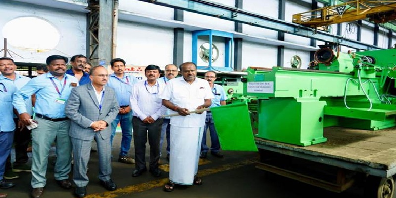
HMT Exports Indigenous Machine Tool to South Africa
Union Minister H.D. Kumaraswamy reviews HMT Kalamassery’s manufacturing capabilities, export growth, modernisation plans and PSU strengthening efforts.
Read moreOther Industrial Products

Warehousing: Enabling Make in India by Boosting Manufacturing Ecosystem
Efficient warehousing is crucial to strengthening India’s manufacturing ecosystem under the Make in India initiative, enabling scalability, competitiveness, and global supply chain resilience, say..
Read moreElectrical & Electronics

Localisation to boost India’s electronics industry: Vijay Aditya Raghavan
In this interview, Vijay Aditya Raghavan, VP – Operations EMS & Head – New Business Initiatives at TVS Electronics, elaborates on the country’s increasing electronics manufacturing capabilitie..
Read moreRelated Products

Ultra-slim Humidity/temperature Indicator With Large 4” Display
ELECTRICAL & ELECTRONIC EQUIPMENT
Countronics offers a wide range of ultra-slim humidity/temperature indicator with large 4” display – Model 7100-4W.
Read more
Integrated Electric Gripper S Series
ELECTRICAL & ELECTRONIC EQUIPMENT
IBK Engineers Pvt Ltd offers a wide range of integrated electric gripper S series.

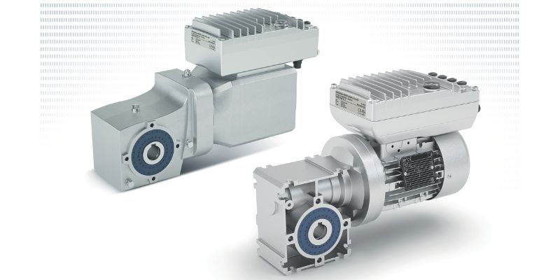
Geared Electric Motors
ELECTRICAL & ELECTRONIC EQUIPMENT
Delco Fans Pvt Ltd offers single phase capacitor run and three
phase geared Instrument motors, totally enclosed face/foot mounted.
latest News
Subscribe to iNoW
For Industry News on WhatsApp, Give a Miss Call on: +91 84228 74016