


Schedule a Call Back


Simulation Technology for PCB Design
Simulation Technology for PCB Design
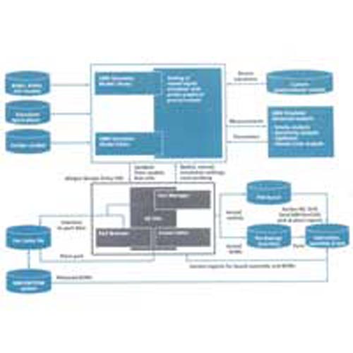
Cadence Design Systems India offers simulation technology for PCB design that integrates seamlessly with the Cadence front-to-back PCB design flow, making it possible to have a single, unified design environment for both simulation and PCB design. The simulation technology allows for automatic identification of analogue and digital signals, and applies A-to-D and D-to-A interfaces. The technology also explores design relationships with 'what if' scenarios before committing to hardware; maximises circuit performance automatically using optimiser. The technology identifies and simulates functional blocks for complex circuitry using mathematical expressions, functions, and behavioural devices. The simulation technology for PCB determines, which components are overstressed using smoke analysis and by observing component yields using Monte Carlo analysis. Offering design entry and editing from a library of more than 18000 symbols and models for simulation design, the technology also helps to access built-in functions that can be described parametrically, or draw piece-wise linear signals freehand with the mouse to create any shape stimulus.
IPF Simulation Technology for PCB Design
Simulation Technology for PCB Design
Simulation Technology
PCB Design Simulation Technology
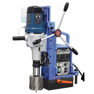
Products from MACHINE TOOLS, POWER & HAND TOOLS Category
Verified
Verified
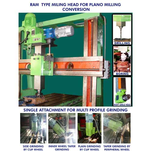
Versatile Machining Capability Through Ram Type Milling & Grinding Heads
Deburring, Drilling, Boring, Tapping and Threading Machines
Verified
Verified