


Schedule a Call Back

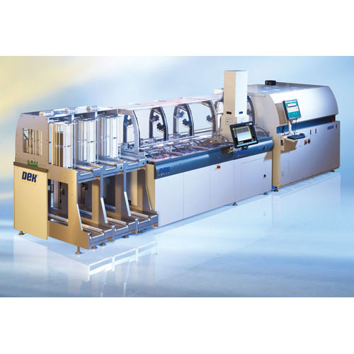
Enhanced Thin Wafer Capabilities

Enhanced Thin Wafer Capabilities
Mass imaging leader DEK is showcasing the company’s new thin wafer processing expertise at the upcoming Semicon West event in San Francisco, California. A full line solution that incorporates a Galaxy Thin Wafer System and a next-generation CHAD WaferMate™ wafer handler, this latest development resolves traditional challenges associated with high-speed handling and processing of thinned wafers on a proven print platform
With the ability to process as many as 60 wafers per hour, the DEK-CHAD technology pairing offers semiconductor specialists a high-volume, high-accuracy thin wafer platform that enables extremely precise printing processes for wafers as thin as 75µm. CHAD’s WaferMate system incorporates advanced engineering principles, delivering thinned and warped wafer handling capability, movement of wafers or paper from a coinstack configuration and the ability to limit wafer contact during transfer to the print pallet so as to avoid any damage to delicate, thinned wafers. Once placed on the DEK thin wafer pallet, which can accommodate wafers as large as 300 mm and is flat to less than 10 µm, the Galaxy transport system precisely and quickly transfers the wafer-loaded pallet into position. Advanced vision capabilities align the wafer and the specified imaging process commences.
Enabled by the superior process capability of the Galaxy Thin Wafer System, today’s most sophisticated packaging techniques including ball placement, DirEKt Coat™ wafer backside coating, protective coating imaging, thermal interface materials deposition, wafer bumping and encapsulation processes can all be accomplished with exceptional accuracy and precision at high UPH. For DirEKt Coat applications, which will be demonstrated at Semicon West, the new Galaxy Thin Wafer System delivers a process capability of Cp>2 @ ±12.5 µm with a Total Thickness Variation (TTV) of less than 7 µm on 200 mm, 150 µm thin wafers for coatings as thin as 25 µm. This unique technology is exponentially faster – by a factor of 10 – than traditional dispensing processes and affords chip footprint maximisation by eliminating the chip fillet. During the live demonstrations, wafer transfer and loading of delicate 120 µm wafers will be carried out by CHAD’s WaferMate handling system.
Commenting on the highly effective DEK-CHAD combination, David Foggie, DEK Semicon and Alternative Applications Manager, explains the technology advantage of the union. “When joined with DEK’s platform approach, which offers packaging firms the ability to incorporate a proven imaging platform to host a variety of processes, the CHAD WaferMate solution affords the custom handling requirements that are often part of the wafer processing equation,” states Foggie. “CHAD’s expertise in secure wafer movement, identification and optical recognition is unmatched and a perfect complement to DEK’s core competency in high UPH materials imaging. This partnership dates back many years and has effectively enabled multiple successful processes at leading global semiconductor firms.”
DEK is a global provider of advanced materials deposition technologies and support solutions including printing equipment platforms, stencils, precision screens and mass imaging processes used across a wide range of applications in electronics pre-placement subassembly, semiconductor wafer manufacture, and alternative energy component production.
CHAD Industries is a pioneer in the area of wafer and substrate handling for WLP (Wafer Level Packaging) applications. Working closely with its customers, CHAD has developed solutions for handling a variety of substrates, from 50 to 300 mm diameter wafers; warped, thin and glass wafers as well as wafers mounted on film frame. The company provides cost-effective solutions by utilising standard robotic platforms and designing in special end-effectors, wafer aligners, cassette tilters, and other custom elements to meet the exact requirements of the specific application.
Product & Technology News
Enhanced Thin Wafer Capabilities
Enhanced Thin Wafer Capability
Enhanced Thin Wafer
Wafer Capabilities
Karen Moore-Watts
Products from Karen Moore-Watts
Verified
Drying Technology for Solar Cell Metallisation
Deburring, Drilling, Boring, Tapping and Threading Machines
Products from MACHINE TOOLS, POWER & HAND TOOLS Category
Verified
Verified
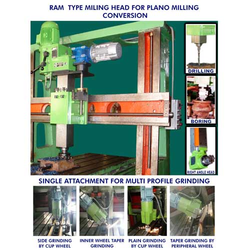
Versatile Machining Capability Through Ram Type Milling & Grinding Heads
Deburring, Drilling, Boring, Tapping and Threading Machines
Verified
Verified