


Schedule a Call Back
Wafer Bonding Solutions

Wafer Bonding Solutions
EV Group (EVG) targets advanced packaging, compound semiconductor and silicon-based power devices, MEMS, nanotechnology and SOI markets with its wafer-bonding, lithography/nanoimprint lithography (NIL), metrology, photo-resist coating, cleaning and inspection equipment. The company offers solutions for permanent wafer bonding. The solutions align with group's wafer-bonding approach, which separates the bond alignment from the bonding step. The solutions utilise high-contact forces under elevated temperatures and a controlled atmosphere, an approach that is also the current process standard. The semi- and automated-wafer bonding systems from the group offer various benefits, including optimal total cost of ownership and real wafer-wedge compensation unit to maximise the bonding yield. The group has an installed base of over 500 bond chambers. The bond alignment systems from EV Group such as the SmartView, can be integrated into a GEMINI Automated Production Wafer Bonding System, which can support sub-micron alignment accuracies. Leveraging its technology strengths to accelerate the success of 3D wafer stacking, the group has developed chip-to-wafer bonding tools for high-yield heterogeneous 3D integration schemes.
Product & Technology News
Products from MACHINE TOOLS, POWER & HAND TOOLS Category
Verified
Verified
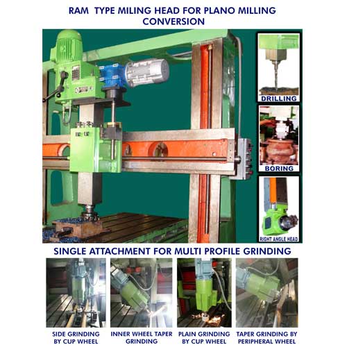
Versatile Machining Capability Through Ram Type Milling & Grinding Heads
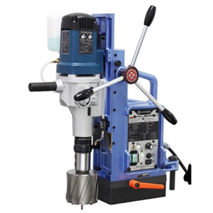
Deburring, Drilling, Boring, Tapping and Threading Machines
Verified
Verified